IBM’s development of copper interconnect for ICs
IBM’s announcement that it had manufactured the first chips with copper interconnect on September 22, 1997, was a press release heard around the world. The images were stunning, as seen in IBM’s photo below. More important was that it marked the successful culmination of a decade-long search for a material to replace aluminum. IBM would ramp copper production in three quarters on its 220nm microprocessors. Everyone knew that aluminum interconnect was running out of steam. As lines shrank, resistance grew, and electromigration (an electron wind that moves molecules like a sand-storm moves mountains) caused circuits to fail. Everyone was working on a solution … most on the wrong solution.
The interesting untold stories center around the decision-making process at IBM and the untruths propagated by the PR machines of the day. One of the hardest things to do in R&D management is to choose which mountain to climb. Otherwise, your resources will be wasted away while researchers try to climb every mountain.
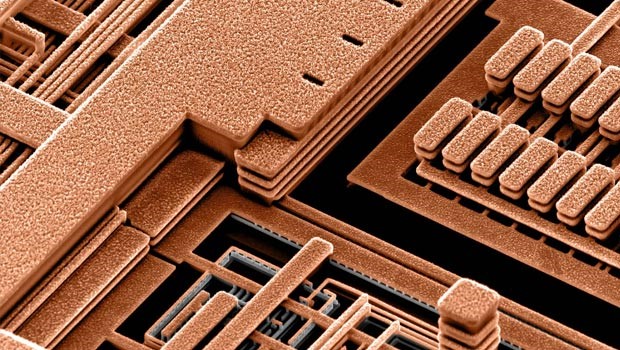
This is one of the most famous technology pictures in our industry, showing the first 3D copper interconnect in microprocessors. Copper to microprocessors was like turbocharges to engines. Source: IBM
The big problem forecast in the mid-to-late 80s was rising RC delay. Half of the problem was rising resistance in aluminum interconnect due to lines getting smaller. The other half was due to coupling between lines due to the high dielectric constant in the SiO2 insulating layers. IBM research management saw this as a two-headed monster. Killing it meant the eventual replacement of both the interconnect and Hi-K dielectric insulator.
The question was, which do you work on and which do you farm out to external research organizations. The answer was simple, as described to me by Bijan Davari at the time: They knew what material would be needed to replace aluminum: copper. They didn’t know what material or process would replace the insulator. Not knowing which material meant it was a much harder problem in physics. Knowing it meant it was a materials engineering problem – much easier to solve. Easier meant cheaper and hence, more of a competitive threat. But the latter was not on IBM’s decision-making agenda.
It is easy to misconstrue that the quick diffusion of IP around copper was a failure on IBM’s part. The problem with this conclusion is that it ignores IBM’s bigger picture of having more to lose than the licensing revenues in terms of corporate profits should system technology not move forward. The industry was very diverse at the time, needing many companies to be brought along for any technology to make it to manufacturing. Without volume, great technologies stay costly, often getting shelved in dusty R&D archives. Moreover, IBM needed copper chips from external suppliers that complemented its microprocessors in its servers. Otherwise, it would have been like putting a modern F1 engine in a Studebaker.
IBM closely managed the rollout of copper tool and materials sales — all technology needed by other chip makers on a scheduled release. Its closest R&D partners were first. Its closest competitors were last. This is partly why AMD was one of the first to implement copper, while Intel one of the last.
This would create some interesting industry relationship fires, the biggest between AMD and Motorola, who had a separate partnership from the one AMD had with IBM. At the time the rest of the industry was barking up the wrong tree — believing MOCVD copper was the way to go. When Motorola announced it had solved the problems with this technology and was moving to manufacturing, AMD knew they were headed for trouble and had to bring them into IBM’s R&D ecosystem.
Very few people held the inside knowledge that the correct process was electroplating. IBM had been the only one to think outside the wafer-fab box. IBM’s insight came from its development of copper electrochemistry for advanced packaging applications. The focus of others was limited to the classic fab technologies of CVD and PVD. Plus, IBM’s deep research expertise at its T.J. Watson Research Center in Yorktown Heights, New York gave it an unmatched ability to move copper interconnect from materials science through materials engineering to production.
For more see: Copper Interconnects-The Evolution of Microprocessors, 20 Years of Cu BEOL in manufacturing, and its future prospects, BEOL Origins, and Copper On-Chip Interconnections