The Chip Insider®
January 15, 2010 – From the Front Lines: The Cook’s Tour: UAlbany NanoCollege and IBM’s R&D Partnering Model revisited… WildPhotons: Deep foundations . . .
The Cook’s Tour: UAlbany NanoCollege and IBM’s R&D Partnering Model revisited.
IBM’s R&D partnering model is one of the great business process innovations of the semiconductor industry. In fact, Dr. John Kelly III won the SIA’s highest honor, The Robert N. Noyce Award in large part due to his persistent efforts, along with that of many others, to develop a viable partnering model that would stem R&D costs. Today, John is a Senior Vice President and Director of Research at IBM, which shows the importance of improving R&D productivity.
IBM’s efforts to build a partnering model for research and development began in 1988, just over 20 years ago, with Siemens and Toshiba in an effort to develop DRAMs. This came on the heels of its pioneering efforts with other industry leaders to develop the first cooperative development models; of which, the results were the SRC and SEMATECH. The difference of the IST alliance was that they would develop a real product that all three could make and sell. Back in the late eighties, the cost of developing a DRAM process had risen to about a billion dollars. Since these were commodities anyway, it made sense to compress what would have been a $3B tab into one. It was a cost sharing approach that benefited supplier and customer alike.
The only real issue was if they could really work together: three different companies and three dramatically different cultures, in an industry known for an ultra-competitive ‘shoot-em out at the OK Corral’ approach. They did make it work and today, IBM’s model has become the gold standard of competitive R&D partnering.
Proof is that they’ve managed to attract some of the best and even some of the strongest companies to participate in applied research that now stretches all the way to manufacturing with their Common Platform alliance. IBM also has numerous group technology alliances where members work to develop particular process technologies, such as this year’s 28-nanometer, low power semiconductor technology platform. IBM’s core technology partners are: Chartered Semiconductor, Freescale, Globalfoundries, Infineon, NEC, Samsung, ST Microelectronics and Toshiba, not to mention the State of New York and more than thirty ecosystem member companies. One fact speaks volumes about the breadth of this alliance: that the cumulative sum of capital expenditures for all the partners accounts for a third of the world’s total.
There is a significant payoff for the companies who participate. A VLSIresearch analysis showed that over this decade, the return for every dollar invested in one of IBM’s competitive partnering efforts has been $2.38 in R&D value.[1] This is why IBM’s R&D partnering model is the most significant new private R&D model to emerge since the Second World War.
In its early days, the College of Nanoscale Science and Engineering’s Albany NanoTech was often dismissed as just being another state-sponsored sandbox. That’s changed, as it has blossomed into a globally respected research center producing both results and students. Today it is a critical part of IBM’s R&D partnering model.
The attraction of Albany NanoTech is about much more than access to technology. It’s also about gaining greater leverage for your R&D dollar. It’s about access to more ideas and more learning cycles. Plus you get to flight-test some of the best engineering students in the world. As one senior executive in Albany NanoTech put it, “If you can dream it, you can do it here.”
The business case for investing in Albany NanoTech is that each dollar spent here is roughly equivalent to four dollars spent in an internal development lab. It doesn’t replace the internal development lab. But it does make your research dollar go much further.
I last did a fab tour here two years ago and there’s been plenty of changes. So let’s go inside the fab and see what’s new:
Like before, Albany NanoTech still has the unique feel of a university environment. It has an excitement and vibrancy to it that is unlike most R&D centers. More interesting this time was the degree to which manufacturing discipline has been brought to bear. If it wasn’t for the lack automation, you’d think it was more of a manufacturing or development center and certainly not a research center.
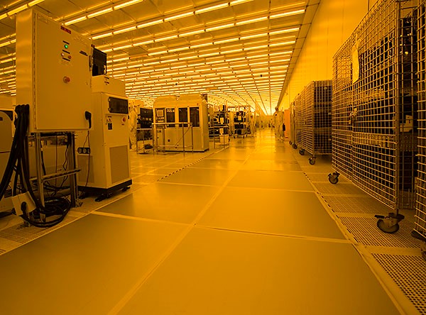
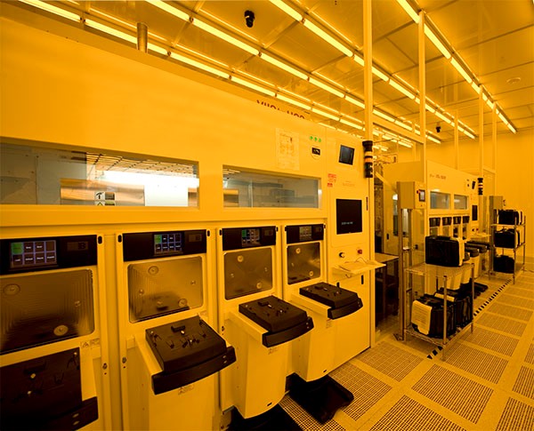
Inside Albany Nanotech: Main Street, which is the main corridor for people, tools and WIP to transverse a fab. IBMalbany09_19
Looking down Main Street, the WIP cages on the right and the lack of overhead transport signal that this is not a development or manufacturing fab. Other than that, the neatness is inspiring. There are not even scuffs on the steel plates that are there to protect the floor for heavy tool installations and deinstalls.
The impression that this facility makes is one of its overwhelming size for a research cleanroom — much less, one that is a university cleanroom. The beauty of mini-environments is that lots of messy and dirty things can happen in a cleanroom without affecting yields. This messiness is an inherent part of every good research environment I’ve been in, as a good researcher learns as much, if not more, from the failures as he or she does from the successes. But unlike most semiconductor research environments, this one is spacious and well equipped. Like Formula 1 racing, you can’t win without the most advanced machines, and a common mistake is to try to win on a Malibu Grand Prix budget. Not so here, as you can see.
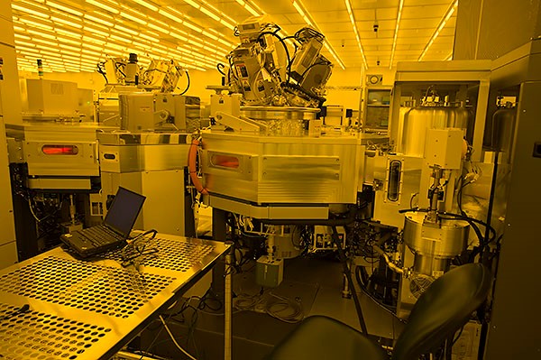
Here’s a good view of a new fab tool being brought to life
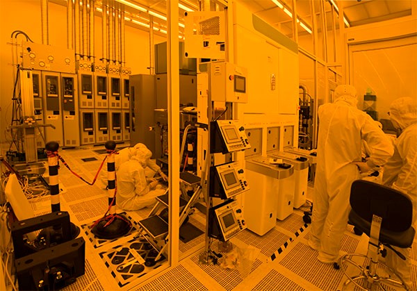
Inside Albany Nanotech: A new tool comes up. IBMalbany09_15
This is no different than what you’d see in a large manufacturing fab. While there is some clutter on the edges, this is very typical of a tool install. More interesting is that this is a state-of-the-art, full-featured, semiconductor production tool. But this tool is also in a research environment, so you can bet there are also plenty of bells and whistles that are not in the OEM’s catalog.
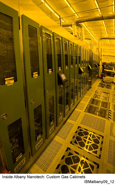
As you look around the fab in the nooks and crannies, there are plenty of signs that things are always being changed to research new technologies. You may recall that chart used in many technology presentations about the increasing number of elements that have been used as the industry has moved from node to node. It shows the periodic table of elements, with the ones used in different colors depending on when they were used. Dealing with the physics of small has meant that we must always look for new materials to make the chips work electrically. The evidence of this can be seen in the rows of gas cabinets, which IBM has custom made.
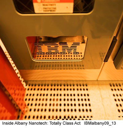
You can tell they are custom made by the fact that the air vents are formed with the IBM logo. It speaks to the high degree of commitment IBM has to getting it right.
Over in the Ion Implant bay, see more full-featured tools. Note in the photo below that each tool has the maximum number of load ports. From a manufacturing viewpoint, this allows IBM to fully debug all parts of a system that will eventually make it to production.
From an R&D perspective, having multiple load ports gives the ability to run multiple test cases efficiently in their own FOUPs. That way the tool can be set-up in a load-and-forget mode. The researcher can keep their project in its own FOUP, load it, and program it to run when the Implanter is available. This frees the researcher and decreases learning cycle time.
Companies who learn faster, get to market faster, and thus, get to money faster. It’s not so much about having the bright idea as it is about getting through the learning cycles needed to get a product to market. Faster learning cycles result in better R&D productivity and ROnR[2].
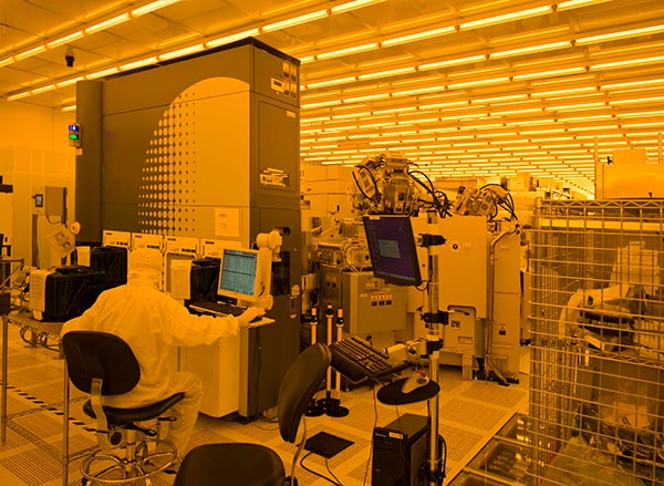
Inside Albany Nanotech: IBMalbany09_07
The fact this fab is not highly automated is another reason for Albany’s vibrancy. Researchers do have to spend more time in the fab than in offices with the carpet dwellers. The result is that you see lots of people from many different organizations always coming and going in this clean room. Yet it still can be very technical. Just look at the back end of this tool and the front of the one below it:
Inside Albany Nanotech: IBMalbany09_05
Inside Albany Nanotech: IBMalbany09_03
Another interesting thing about Albany NanoTech is the degree to which the different suppliers work together. This is the way it’s been since day one and it is fairly unprecedented. I walked freely into and out of one research area and over to another. I talked to the people in each and they were very open about how good this environment was for their company as well as the working environment with competitors. They do stay out of each other’s areas on an honor system. Yet they are not shy about working together informally to solve a common integration problem that affects the customer or just to lend the occasional hand. It’s amazingly collegial for companies who compete fiercely against each other and yet can fiercely work together to help a common customer. I’d call it collegial competition . . . the bottom line is that the people here really work together for the common good. Adam Smith’s invisible hand works here daily.
By G Dan Hutcheson Copyright © VLSI Research Inc. All rights reserved.
[1] Measured on the basis of historic growth trend in R&D expenditures before partnering versus actual expenditures after entering the partnership.
[2] Return On n Years of research.