|
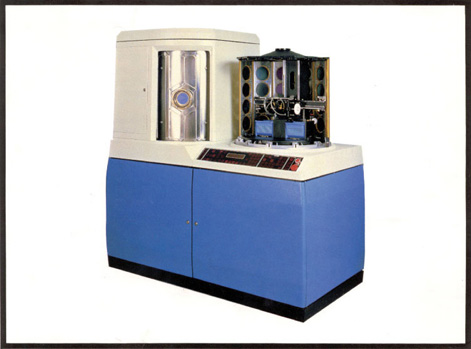 |
It can be said that the AME 8100 launched the
modern era of etching and changed the face of VLSI chip
manufacturing. Prior to this system the industry was struggling with
etch; it was slow and imprecise, and results varied substantially across
the wafer. Yield was abysmal and for etching oxides it was zero—not
absolute but close to it. Most suppliers were trying to convert from
batch etching to single wafer etching to get better results, but that
just slowed things even more.
Bob Graham, then VP of Marketing at Applied, once told me of his
epiphany while visiting Bell Labs. Dan Maydan showed off his new
etcher to Bob, who mistook it as a modified version of the AME 7600.
Bob returned to Applied convinced that batch etching was the way to
go and that they must bring Maydan and his team out to Applied.
Dan brought along David Wang and Sass Somekh. David had tremendous
trouble with oxide etching, always winding up with too much detritus
and ‘grass’—a kind of growth that looked like grass. He eventually
invented a new process that included an organic covering which
eliminated most of these problems.
Nine months after introducing the AME 8100, Applied Materials emerged
out of nowhere as the largest supplier of etch machines in the
world.
|